program
The 2027 program will be posted later this year.
Download the 2025 GOMACTech Mobile App


Agenda
PROGRAM BOOKLET FULL CONFERENCE AT A GLANCE tuesday Plenary schedule
Keynote Speakers
Microelectronics Commons: The New Battleground of Global Motorsport
This insightful overview contemplates the progression and development of microelectronics in auto racing, ranging from the more traditional platform of INDYCAR racing into the rapidly growing, fully sustainable, and all-electric FIA Formula E World Championship. Learn from a leader in the motorsports industry about how involving regulations and increased technology integration has led to software development being the new trackside weapon, both on and off the racetrack.

Roger Griffiths
Team Principal
Andretti Formula E, Andretti Extreme E
Having joined Andretti in the spring of 2014, Roger Griffiths serves as the team principal for Andretti Formula E and Andretti Extreme E. Griffiths’ vast background in many motorsports endeavors including Formula One, INDYCAR, American Le Mans Series, European Le Mans Series, and Super Touring Cars, Griffiths has led Andretti Formula E to 10 wins and 32 podiums across nine seasons. He also served as the technical director for Honda Performance Development, where he experienced success at the Indy 500 in 2012 and the 2013 Driver’s Championship. The UK native is an engineering graduate of Loughborough University of Technology (1991) and the year following his graduation, Griffiths earned his master’s degree in automotive product engineering at Cranfield Institute of Technology with a specialization in vehicle modeling and lap simulation.
More than Microchips
Whitney Mason
Director
Microsystems Technology Office (MTO)
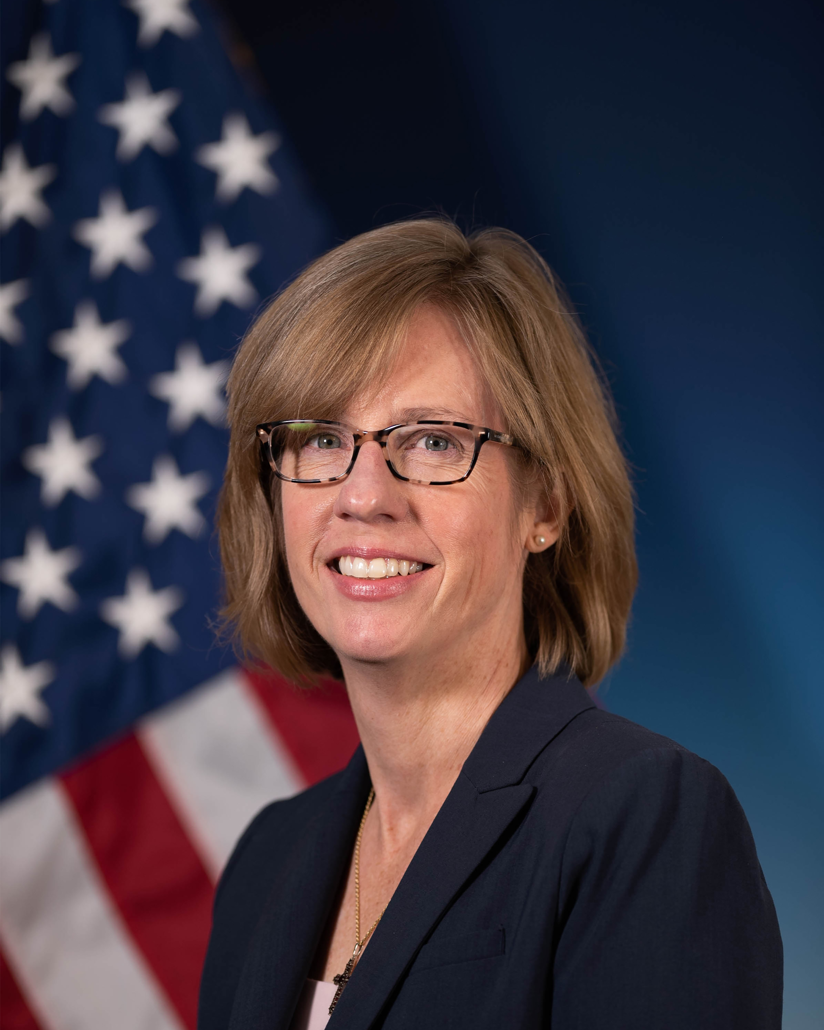
Since the invention of the transistor in 1947 and the integrated circuit in 1958, microchips have fueled scientific advancements, manufacturing innovations, and economic growth for most of the modern era. Today, DARPA’s Microsystems Technology Office (MTO) will advance the next generation of microsystems to disrupt the underlying technology, disrupt current manufacturing, and create new markets. This disruption requires unique insight to discover fundamentally new ways of creating advanced circuits that will dramatically alter and exceed the current state-of-the-art in microsystems. This will involve using the power of light at the microscale in three dimensions with advanced photonics. It will involve harnessing quantum mechanical phenomena for sensors and computers that break traditional classical limits. It will involve developing a toolbox of organic and biological molecules and hybrid bioelectronics that will exploit living system phenomena and connect back to traditional microsystems. Finally, it will involve developing technologies to affordably, rapidly, and sustainably fabricate these and other microsystems to lead to a new domestic manufacturing ecosystem that will exploit commercial scaling and underpin strong domestic economic growth.
Whitney Mason is the director of the Microsystems Technology Office (MTO). Previously, she held the deputy director role in the agency’s Strategic Technology Office (STO) from June 2022 to October 2023. Prior to joining STO, Dr. Mason served as a program manager in MTO from November 2017 to May 2022. Her research interests include imaging sensors that provide multifunction capability. In particular, she is interested in novel device structures, optics, and electronics that enable new capabilities compared to current state-of-the-art imaging systems. Dr. Mason joined DARPA from the Army C5ISR Center, formerly the Army Communications-Electronics Research, Development and Engineering Center, where she was the director of the Science and Technology Division within the Night Vision and Electronic Sensors Directorate at Fort Belvoir, Virginia. In that role, she led a team of scientists and engineers in the pursuit of new and improved focal plane array materials and devices; advanced read-out circuits; and enhanced optical materials and designs, lasers, and image processing. Dr. Mason holds a doctor of philosophy degree in physics from the University of Oklahoma and a bachelor of science degree in physics from Georgetown University.
Jack S. Kilby Lecture Series
Advanced R&D for Mission Needs

Dr. Joshua Fryman
Intel Fellow, Head
Intel Government Technology R&D Group
Dr. Joshua Fryman is an Intel Fellow and heads Intel Government Technology’s R&D group, setting the strategy and priorities for all external R&D between Intel and Public Sector sponsor agencies or commercial entities. He joined IGT from the Office of the CTO under Greg Lavender.
Prior to his role in IGT, his work was primarily focused on applied R&D for commercial and government customers, focusing on problems that are 3-10 years out on the horizon. Throughout his career, Dr. Fryman has been engaged in multiple project types, from fabricating and testing circuits to designing microprocessor and system architectures, interconnects, packaging, compilers, runtimes, applications, and algorithms.
In his role as Chief Architect or Principal Investigator (PI), Dr. Fryman has led pre-exascale programs such as DARPA UHPC and DOE Fast Forward and Xstack. He has also played a pivotal role as PI for at-scale future AI and analytics programs such as DARPA HIVE, IARPA AGILE, and DOE’s Advanced Memory Technology efforts. His role as a PI also includes security programs such as DARPA GAPS and other appliances.
Dr. Fryman obtained his BS in Computer Engineering from the University of Florida and a PhD in Computer Architecture from Georgia Tech. Renowned for his insights in the field, he is a frequently invited speaker on microelectronics, systems, packaging, integration, and hardware-software co-design topics.
The NSTC: Leveraging Public-private Partnerships to Advance U.S.-led Semiconductor R&D, Workforce, and National Security

Program Management Office
Natcast
The National Semiconductor Technology Center (NSTC) is a public-private consortium established by the CHIPS and Science Act and is dedicated to semiconductor R&D in the United States. Operated by Natcast, the NSTC convenes industry, academia, and government from across the semiconductor ecosystem to address the most challenging barriers to continued technological progress in the domestic semiconductor industry, including the need for a skilled workforce. Natcast Program Management Office Director Salman Nasir shares insights into the once-in-a-lifetime opportunity presented by the NSTC, its activities to-date, and its impact on innovation, workforce, and economic and national security.
Mr. Salman Nasir is the director of the Program Management Office at Natcast, overseeing R&D programs. Previously, he was the Programs & Site Lead at Battelle's Dayton facility, managing Microelectronics Security Research and Hardware Assurance programs. He has over a decade of R&D experience particularly in microelectronic hardware, RF communication, EO/IR sensors, high-performance computing, and image processing. Mr. Nasir holds an MBA, an MS in Electrical Engineering, and a BS in Electrical Engineering. Mr. Nasir is a certified PMP® and Six Sigma Black Belt, with multiple industry and DoD awards, including the Defense Manufacturing Technology Achievement Award.
DoD Microelectronics – Transitioning Innovation in 2025 and Beyond

Dr. Carl E. McCants
Special Assistant to the Director
Darpa
In the March 2024 “National Strategy on Microelectronics Research” published by the Subcommittee on Microelectronics Leadership of the National Science and Technology Council,1one of the four goals and objectives is “Create a Vibrant Microelectronics Innovation Ecosystem to Accelerate the Transition of Research and Development to U.S. Industry”. This goal “is focused on the entire R&D landscape and presents strategies and actions to create a vibrant microelectronics innovation ecosystem to… support actions at each stage of the microelectronics technology development pathway… to build a virtuous cycle of microelectronics innovation.”2 The DoD faces unique challenges in developing, accessing, and utilizing microelectronics design, fabrication, packaging and assembly, characterization, and failure analysis capabilities needed to maintain and extend technological leadership in national security applications. This talk will explore the question “How should the DoD microelectronics ecosystem change to leverage and transition innovative capabilities that keep pace with or create the state of the art?”
[1] https://www.nitrd.gov/pubs/National-Strategy-on-Microelectronics-Research-March-2024.pdf
[2] https://www.nitrd.gov/pubs/National-Strategy-on-Microelectronics-Research-March-2024.pdf p.vi.
Dr. Carl E. McCants is a special assistant to the DARPA director, focusing on efforts to inform microelectronics policy and national strategies for microelectronics research and development.
Prior to his role at DARPA, he was the technical director of the Supply Chain and Cyber Directorate of the National Counterintelligence and Security Center (NCSC), in the Office of the Director of National Intelligence and a senior program manager at the Intelligence Advanced Research Projects Activity (IARPA).
From 2010 to 2012, he was a program manager in the Microsystems Technology Office at DARPA, focused on microelectronic integration and hardware assurance and reliability. From 2003 to 2009, he served as the chief technologist to the director of MTO, and special assistant to the DARPA deputy director.
From 1999 to 2003, McCants was a project manager at Agilent Technologies’ Semiconductor Products Group, and from 1988 to 1999, he was a development engineer at Hewlett-Packard’s Optical Communication Division.