program
Download the 2024 GOMACTech Mobile App
The GOMACTech mobile app includes everything you need to navigate GOMACTech 2024: sessions, schedules, and much more. Download it now and don’t miss a moment of GOMACTech:


Agenda
Community and Collaboration
The 2024 preliminary program and conference at-a-glance are now available below. Please note that program and content are still under development.
Charleston Area Convention Center Map
2024 TECHNICAL PROGRAM 2024 conference at-a-glance 2024 FULL CONFERENCE AT-A-GLANCE program bookletWorkshops
Trusted Supplier Industry Day
Monday, March 18
8 am – 5 pm
The thirteenth Trusted Supplier Industry Day will be an interactive event with an opportunity for all attendees to hear from key leaders and provide input on the critical issues facing our community. We have seen tremendous change since last year’s Industry Day. The CHIPS Program office has begun funding projects under the CHIPS and Science Act for the construction, expansion, or modernization of commercial facilities for the fabrication of leading-edge, current-generation, and mature-node semiconductors. DoD announced in August the eight Microelectronics Commons hubs that will form a national network to create direct pathways to commercialization for US microelectronics researchers and designers from “lab to fab”, and in December announced the project areas in which hubs can propose projects to be funded. The Industry Day program will feature speakers who will address these areas and topics including evolving microelectronics strategies with a focus on security and integrity. Speakers will also address developments regarding the CHIPS Research and Development Office’s National Semiconductor Technology Center as well as the National Advanced Packaging Manufacturing Program (NAPMP) Advanced Packaging Piloting Facility (APPF) where successful advanced packaging innovation development efforts will be evaluated and validated for scaled transition to U.S. manufacturing. The Industry Day is being designed to provoke thoughtful conversations and up-to-date information on the many activities being pursued to restore U.S. leadership in semiconductor manufacturing with a semiconductor supply chain that considers security along with technical performance. Please join us on March 18th to add your voice to the discussion of the most critical electronics issues of the day.
Microelectronics Assurance Workshop
Agenda
Monday, March 18
8:30 am – 5 pm
Microelectronics Assurance is one of the key technical execution areas (TEA) under the OUSD(R&E) Trusted & Assured Microelectronics (T&AM) program. The Microelectronics Assurance TEA (MAT) meets the needs of key stakeholders to ensure the confidentiality and integrity of microelectronic components used in DoD systems by providing hardware assurance and vulnerability assessments; FPGA supply chain lifecycle assurance; microelectronics supply chain risk and threat assessments; and the development of best practices guidance, assessment tools, technologies, techniques, and mitigations. MAT leverages the expertise and services provided by the Joint Federated Assurance Center (JFAC) Hardware Assurance Labs to meet the goals and objectives of MAT.
On-shore Advanced Packaging Capabilities
Agenda
Monday, March 18
1:00 – 4:30 pm
The government Reshore Ecosystem for Secure Heterogeneous Advanced Packaged Electronics (RESHAPE) and Defense Production Act Investment (DPAI) teams will present overviews of currently funded on-shore advanced packaging capabilities. Program overviews, interactive discussions, and presentations from vendors on their advanced packaging manufacturing capabilities will provide an opportunity for attendees to hear from key stakeholders and provide input on the critical issues facing the advanced packaging community. Awards have been made through the Industrial Base Analysis and Sustainment (IBAS) program, RESHAPE effort, to Osceola County Fl/Skywater/BRIDG and Micross Components. The DPAI program has awarded Calument and GreenSource Fabrication LLC. Speakers will address key needs and developments in packaging to include Fan-Out Wafer Level Packaging (FOWLP), Wafer Prep and High-Density Interconnent/High Density Build-up (HDI/HDBU). Please join us on the afternoon of March 18th to hear the latest in government packaging capability investments and be part of the needs and challenges discussions for this advanced packaging community.
Panel Discussions
DoD Workforce Development Accomplishments and Future Directions
Wednesday, March 20
10:30 am - 12:10 pm
There is a big push on workforce development (WFD) in the CHIPS Act to address the gaps identified by the various trade organizations. USG and DoD programs are unable to meet staffing goals for domestic, clearable microelectronics engineers. The Scalable Asymmetric Lifecycle Engagement (SCALE) program continues to assess and aggregate the stakeholders’ needs and provide data-driven microelectronics workforce recommendations. The DoD focus areas cover radiation-hardening, heterogeneous integration/advanced packaging, system on a chip, embedded system security/trusted AI, supply chain awareness, and others. The panel will discuss who is responsible for WFD, possible standards, and how the progress is measured. It will look at different groups as post-secondary, kindergarten-12, and others. There is need to grow the research work force to use the key microelectronic investments.
STEM the “Leaky Pipeline”
Wednesday, March 20
1:30 - 3:10 pm
Studies show that women and underserved populations leave the STEM workforce at significantly higher rates, which is of particular concern as USG and DoD programs are unable to meet staffing goals for domestic, clearable microelectronics engineers. Human resources initiatives alone have not been able to STEM the “leaky pipeline”. It is time to take the problems to the engineers. Peers, technical leads, and managers have a greater impact on the daily experience of the individual engineer than yearly company mandated trainings. The engineering community must own this problem and find the solution. This panel features conversation between members from government, academia, and industry to explore hidden barriers to employee growth and retention while seeking actionable quantifiable solutions. Panelists will share experiences with programs aimed at career development for underserved populations. The panel will identify strategies for enhancing systems for items such as program technical effort, performance evaluations and work allocation, as well as quantitative methods used to evaluate initiatives aimed at improving workforce equity.
Leveraging Startup Innovation within the DoD Microelectronics Community
Wednesday, March 20
3:30 - 5:10 pm
Small companies that are new to working with the USG often do not have the resources to effectively share their perspectives with government decision-makers and struggle to identify relevant funding opportunities within active research and development (R&D) initiatives. Such companies play a critical role in driving rapid innovation and fueling economic growth. As the microelectronics ecosystem has become more complex, closer collaborations between all stakeholders are critical to maintaining access to the best technology in the industry. The panel will focus on domestic startups and emerging small- and mid-size microelectronics companies with discussion surrounding how such companies can more actively participate within major government-funded R&D initiatives, such as the CHIPS Act. The panel will provide perspectives from small commercial companies and USG government stakeholders, and discuss challenges they face, how they can impact the community, and how to better leverage such companies for USG microelectronics needs and to bolster domestic capabilities.
STEM the “Leaky Pipeline” Part II
8:30 am – 10:10 am
Thursday, 21 March Join us Thursday morning as we offer a recap of the Wednesday panel in which we discussed concrete ideas to grow and retain women and underserved populations in the defense microelectronics workforce. Make connections and share ideas for next steps, including coordination with workforce development initiatives and quarterly working groups. It’s time to make progress in our workplaces and our industry.
The T&AM MPW Program Panel Discussion
Thursday, March 21
10:30 am - 12:10 pm
The Trusted and Assured Microelectronics (T&AM) Program within OUSD Research and Engineering (R&E) aims to provide the U.S. warfighter with the state-of-the-art (SOTA), assured microelectronics required to meet DoD system modernization goals. One of the primary objectives of the program is to enable access to commercial industry and government to develop and demonstrate SOTA designs that advance DoD initiatives. T&AM sponsors multi-project wafer (MPW) run opportunities to enable access to SOTA US commercial foundries ≤ 22nm in support of the DoD microelectronics goals and to aid in developing specific foundation and functional intellectual properties. Currently, T&AM sponsors MPW opportunities with GlobalFoundries and Intel Foundry Services. The program is available to relevant designs from the defense industrial base (DIB), government laboratories, and academia. The panel will provide an overview of T&AM MPW opportunities and a discussion of technologies currently sponsored.
Keynote Speakers
Tuesday, 19 March, Ballroom AB
Keynote Address I
8:45 – 9:30 am

Dr. Jay Lewis
Director of the National Semiconductor Technology Center (NSTC) Program
CHIPS R&D Office at the Department of Commerce
“A Vision for Innovation Through Collaboration in the National Semiconductor Technology Center (NSTC)”
This address discusses a variety of challenges in the microelectronics ecosystem, and how NSTC can unite the community to address those challenges. Some of these are technical – logic, mixed signal, memory, photonics, design/co-design, and architecture all need new breakthroughs to continue to advance the state of technology. Others are ecosystem challenges. Access to design tools, IP, and collaboration environments, as well as increasing use of AI in design and verification flow will all transform the way that the industry does its work. Access to advanced R&D facilities and leading-edge shuttles can accelerate the pace of research. The traditional venture model has been mismatched with hardware investments for decades, and this has been a drag on innovation, but there are new ideas for how this can work better. In closing, we will provide updates on the priorities for this year, and show how the NSTC can change the long-term trajectory for innovation.
Keynote Address II
9:30 – 10:15 am

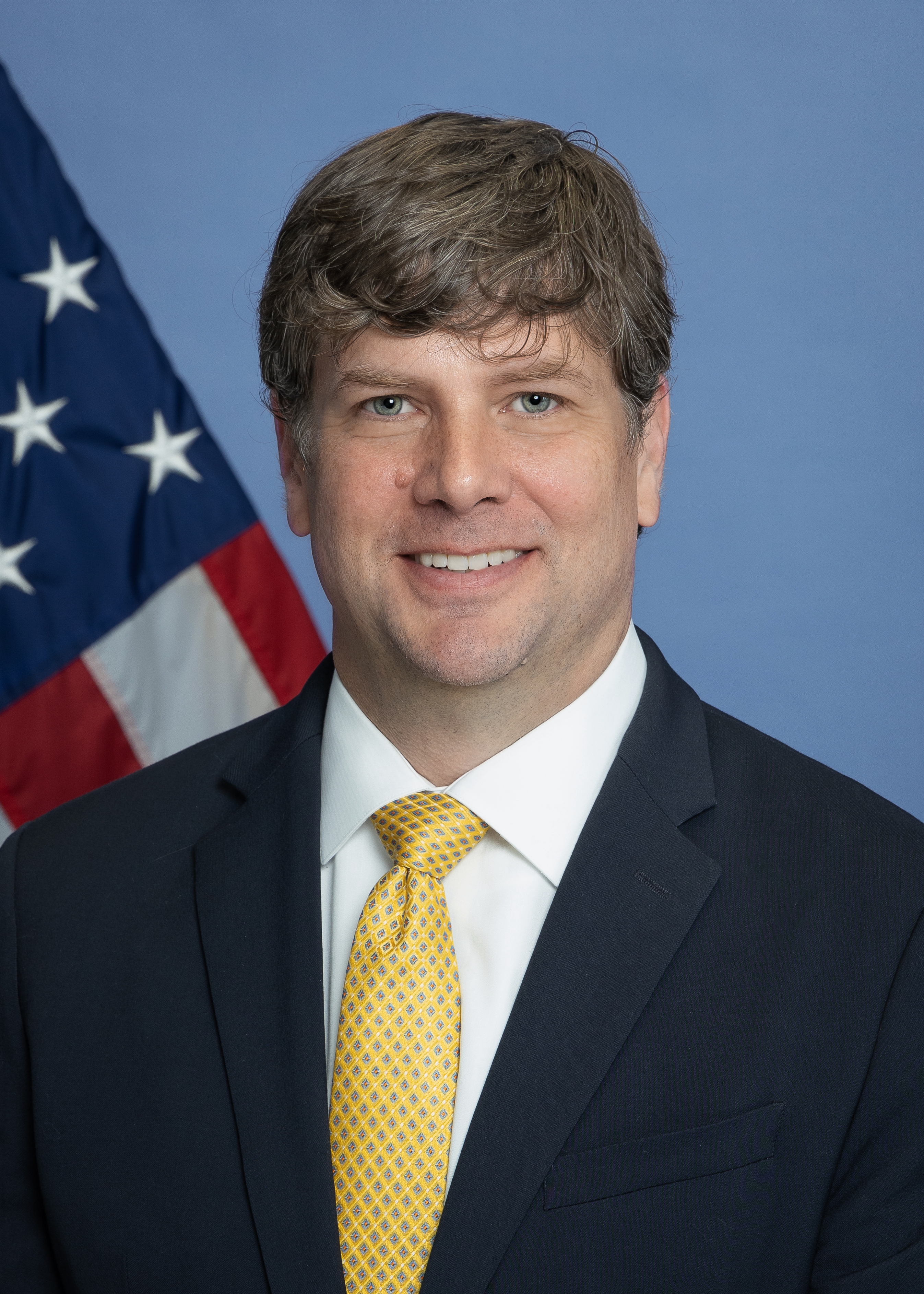
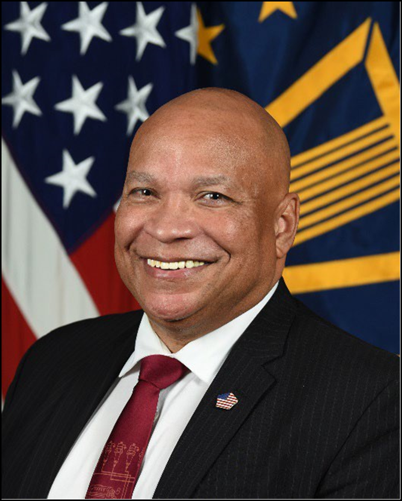
Assistant Secretary of Defense for Critical Technologies
Office of the Under Secretary of Defense for Research and Engineering
“DoD Microelectronics Overview”
This keynote will emphasize and remind the community of the importance of securing microelectronics that are crucial to multiple critical infrastructure technologies, including those that directly impact our country’s security and defense. Featured issues include key microelectronics initiatives championed by our federal government and within the Department of Defense (DoD) to illustrate a whole-of-government approach. The presentation will include highlights of the speaker’s critical technology portfolio as well as some of the challenges DoD faces while seeking collaborations with industry.
Keynote Address III
10:30 -11:15 am

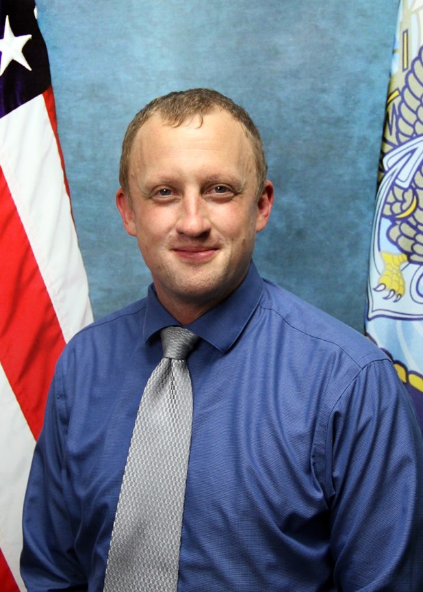
Acting Program Manager
Advanced Materials and Manufacturing Technologies Office (AMMTO)
U.S. Department of Energy (DOE)
“Microelectronics Energy Efficiency and Power Electronics for Zero Carbon”
This brief overview of micro- and power electronics research at the US Department of Energy will also describe how AMMTO intends to lead DOE’s power electronics efforts to achieve net zero carbon with a P.E. Roadmap that enables accelerated deployment of clean energy technologies, the net zero carbon grid, and electrified transportation and industry. Additional focus includes the “Microelectronics Energy Efficiency Scaling for 2 Decades” (EES2) initiative. The goal of this talk is to inspire the community about the EES2 and other microelectronics and power electronics work at the DOE and to provide information about how everyone can contribute.
Jack S. Kilby Lecture Series
Tuesday, 19 March, Ballroom AB
Kilby Address I
11:15 – 11:45 am

Acting Technical Director
Microelectronics Commons
“Microelectronics Commons: A National Network for Defense Microelectronics Innovation”
The Microelectronics Commons (Commons) is a key national initiative that is executed with oversight from the Office of the Under Secretary of Defense for Research and Engineering’s (OUSD(R&E)’s) Principal Director for Microelectronics as part of the CHIPS and Science Act. This effort benefits both the Department of Defense (DoD) and the United States in spurring development of a domestic microelectronics manufacturing industry by forging critical partnerships with commercial industry, academic, and government partners within eight regional hubs across the country. The Commons supports the acceleration of laboratory to fabrication (lab-to-fab) prototyping through hubs to create a network focused on maturing emerging microelectronics technologies, strengthening microelectronics education and training, and developing a pipeline of talent to bolster local semiconductor economies and contribute to the growth of a domestic semiconductor workforce. In particular, the Commons will address the need for processes, materials, devices, and architectures to be developed and transitioned from research labs to small-volume prototyping in a fab or foundry. The Microelectronics Commons released the first annual Call for Projects (CFP) in December 2023 and released 41 topics across six technical areas: Electronic Warfare, Commercial Leap Ahead, AI Hardware, Quantum, Secure Edge/Internet of Things and 5G/6G. This talk will provide an update on the progress in spurring advances.
Kilby Address II
11:45 am – 12:15 pm

Director
National Advanced Packaging Manufacturing Program
(on assignment from UCLA)
“Packaging: Then, Now and in the Future”
In 2014, Dr. Iyer gave a Kilby Lecture at this conference where he outlined at a very exploratory level the promise of packaging to move Moore’s law from a “scale the chip play “to a “scale the system play”. Ten years later, things have certainly taken off and those rudimentary concepts that he discussed, such as finer package pitches, simpler communication protocols, three-dimensional stacking, and chiplet concepts have made a significant impact in our ability to build both high-performance and low-power systems that are the very foundation of our incredible current AI/ML and telecommunication capabilities. However, we have barely scratched the surface as far as the incredible potential of advanced packaging. This talk will offer a roadmap for advanced packaging (that was funded by NIST) and a strategic vision of how the NAPMP will implement this roadmap in a manner that allows for the introduction of on-shore manufacturing of advanced packaging and true heterogeneous integration, in not just the high-performance and low-power arenas, but also in the all-important application of medical electronics.